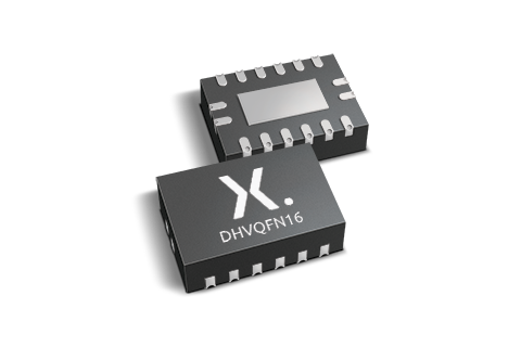

The NCA9306-Q100 is a 2 channel bidirectional I2C and SMBus multi-voltage level translator with an enable (EN) pin input. It allows voltage translation between 0.95 V and 5 V without the use of a direction pin. It supports up to 100 MHz up translation and >100 MHz down translation at ≤ 30 pF capacitive load. There is no need for a direction pin which minimizes the system effort.
Automotive product qualification in accordance with AEC-Q100 (Grade 1)
Specified from -40 °C to +125 °C
2-channel bidirectional voltage translator for SDA and SCL lines in mixed mode I2C bus applications
Open-drain I2C-bus I/O ports (SCLA, SDAA, SCLB and SDAB)
Provides bidirectional voltage translation with no direction pin
High-impedance SCLA, SDAA, SCLB and SDAB for EN = LOW
Up translation
< 100 MHz; CL = 30 pF
< 40 MHz; CL = 50 pF
Down translation
> 100 MHz; CL = 30 pF
< 40 MHz; CL = 50 pF
Hot insertion
Bidirectional voltage level translation between:
0.95 V and 1.8 V, 2.5 V, 3.3 V and 5.0 V
1.2 V and 1.8 V, 2.5 V, 3.3 V and 5.0 V
1.8 V and 2.5 V, 3.3 V and 5.0 V
2.5 V and 3.3 V and 5.0 V
3.3 V and 5.0 V
Low standby current
5 V tolerant I2C-bus I/O pins to support mixed mode signal operation
Low RON provides less signal distortion
Latch-up performance exceeds 100 mA per JESD78 class II level A
ESD protection:
HBM ANSI/ESDA/JEDEC JS-001 Class 2 exceeds 2000 V
CDM ANSI/ESDA/JEDEC JS-002 Class C3 exceeds 1000 V
GPIO, MDIO, PMBus, SMBus, SDIO, UART, I2C, and other interfaces in Telecom infrastructure
Industrial
Personal computing
Router and Industrial Automation
| Type number | Product status | VCC(A) (V) | VCC(B) (V) | Logic switching levels | Output drive capability (mA) | tpd (ns) | Nr of bits | Power dissipation considerations | Tamb (°C) | Rth(j-a) (K/W) | Ψth(j-top) (K/W) | Rth(j-c) (K/W) | Package name |
|---|---|---|---|---|---|---|---|---|---|---|---|---|---|
| NCA9306DC-Q100 | Production | 0.95 - 5.0 | 0.95 - 5.0 | CMOS | n.a. | 0.4 | 2 | low | -40~125 | 206 | 36.1 | 117 | VSSOP8 |